Design of the system
Overview
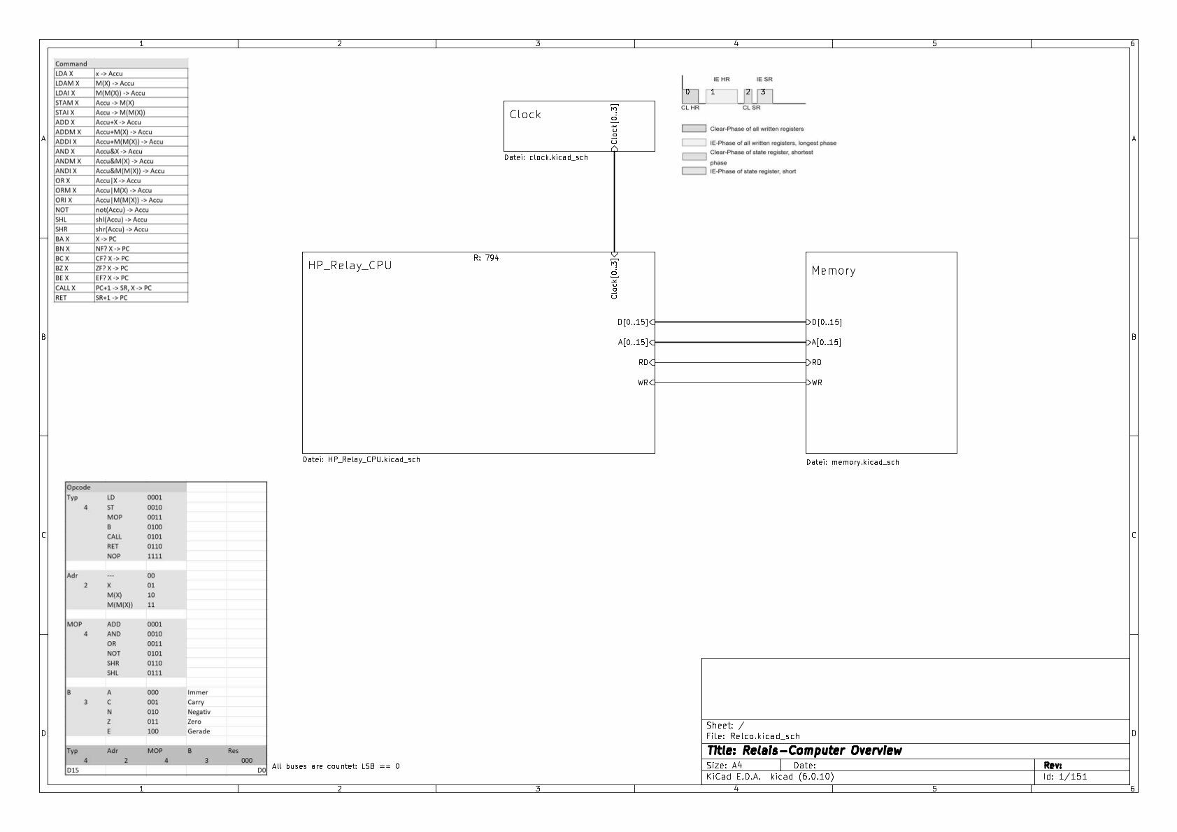
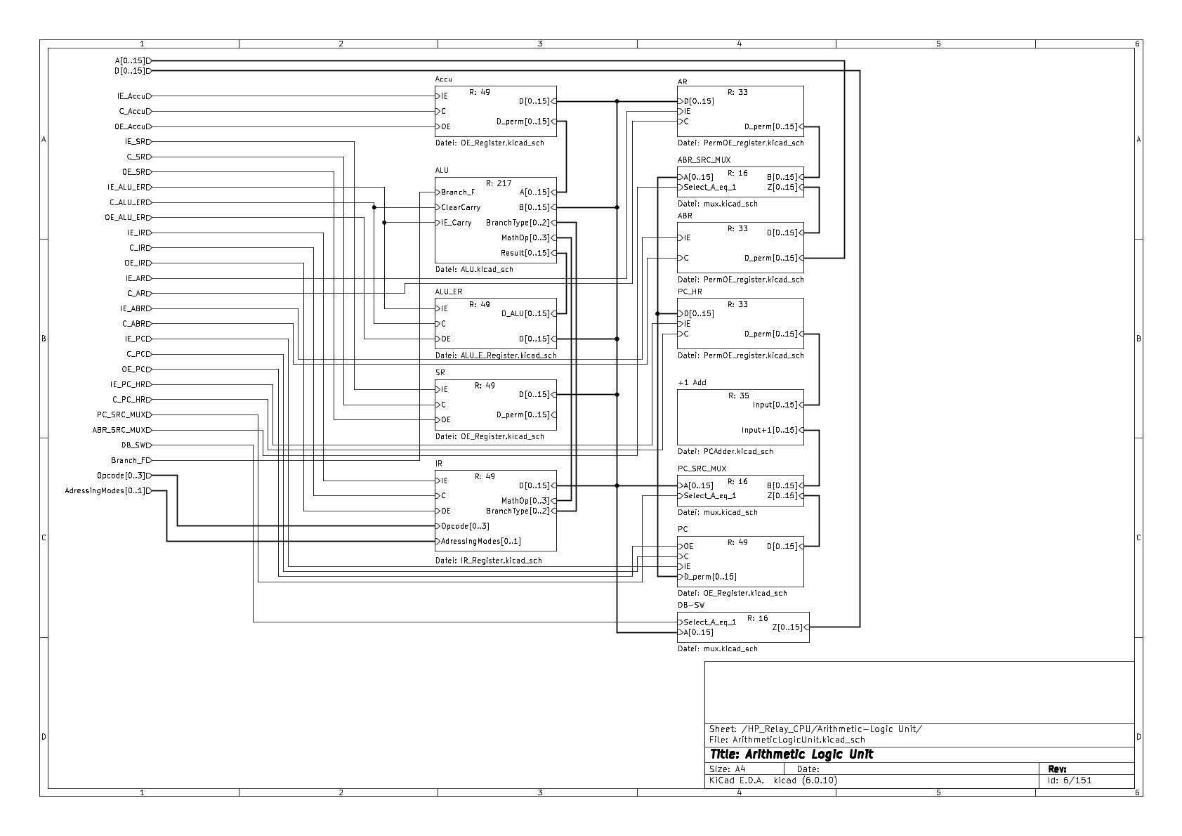
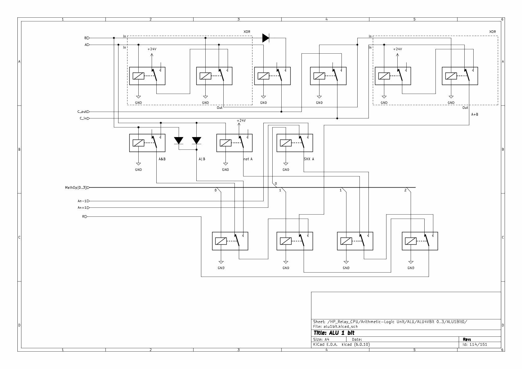
The system ist a very simple CPU using an Accu register like CPUs in the 80s. All mathematical operations are using the Accu, also all store / load operations. And, because it is a "High Performance" relay system, the program counter has its own adder which is only able to add 1 to the program counter.
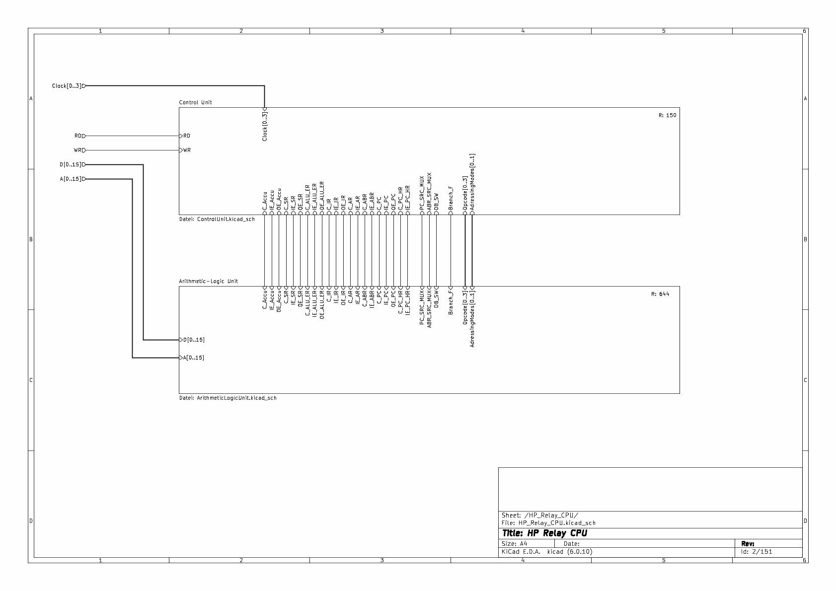
The following diagram shows an overview about the system structure:
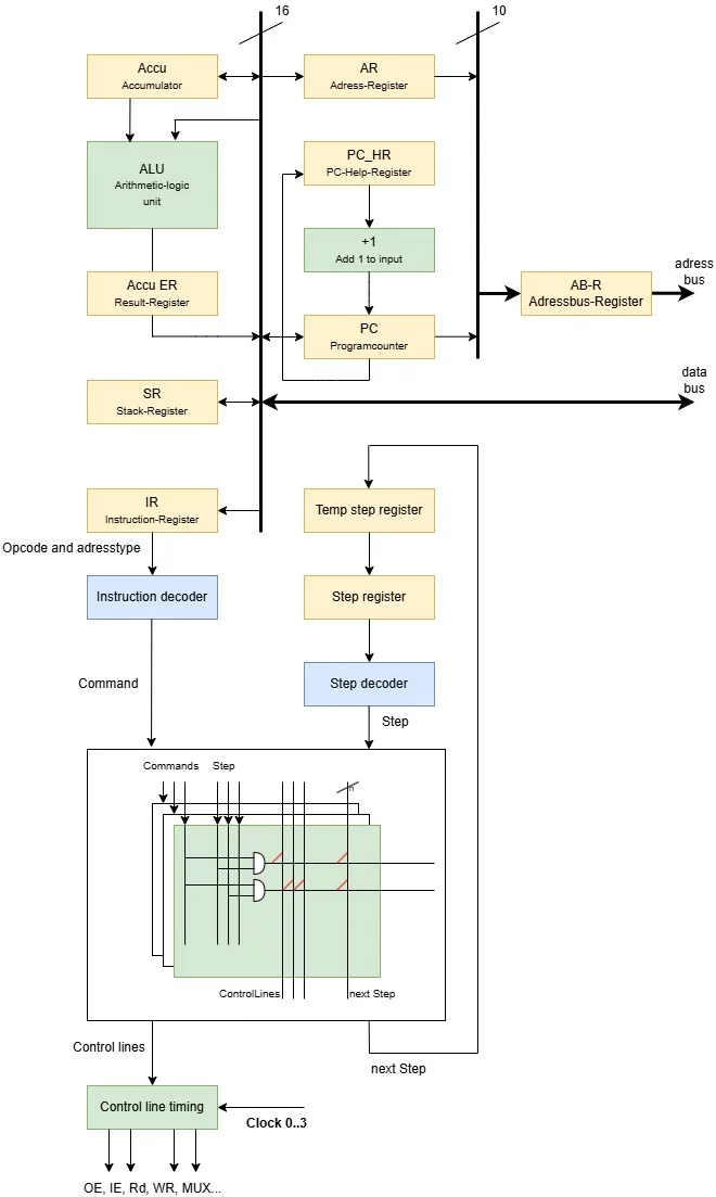
Note: The PC_HR register is necessary, because I can not write the changed PC based on its own value plus 1 direct into the PC...
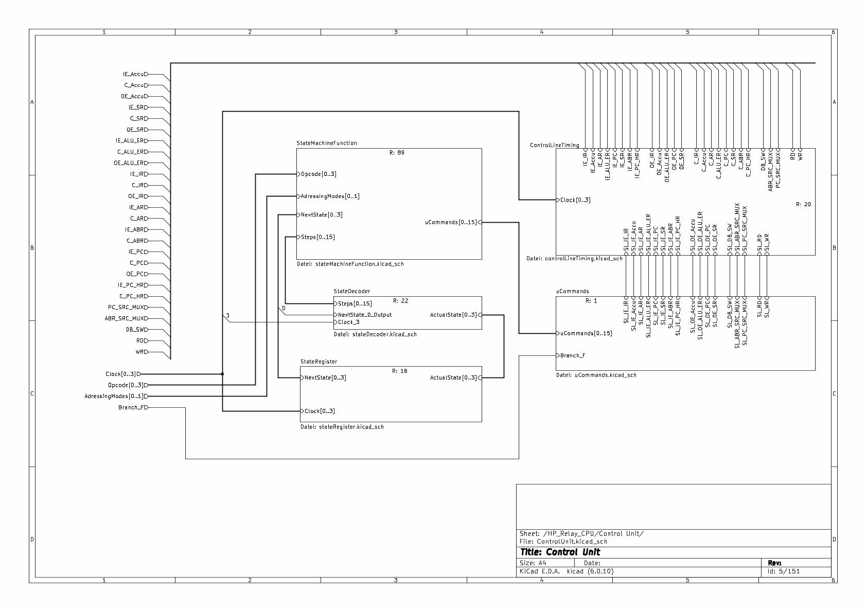
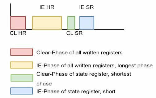
One detail is important to understand the design of the system: all registers, which are realized by "self retaining" relays, have to be cleared before any information can be stored, also before the stored information can be changed. Thats the reason why the clock of the system is not an ordinary clock as you know it from digital systems. The clock of this system consists of 4 different
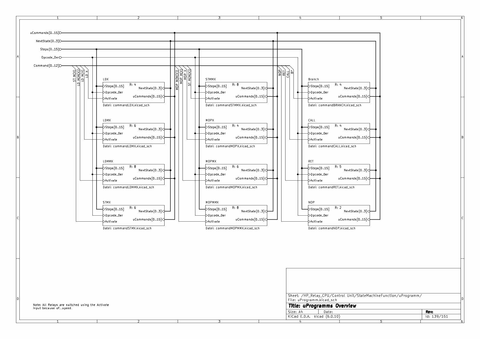
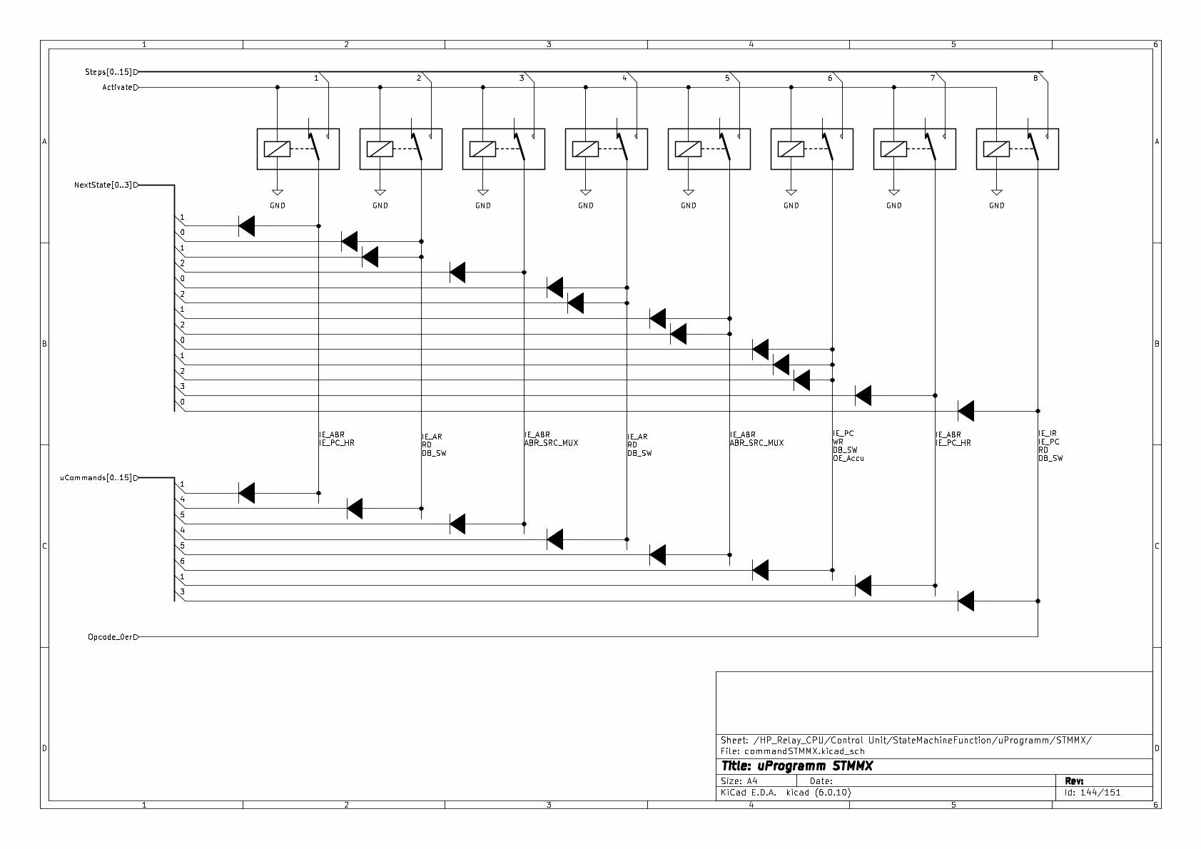
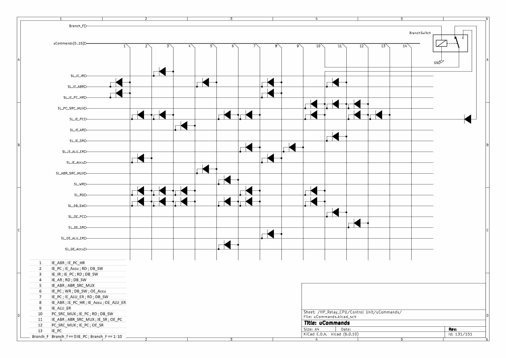
The control unit of the system is using the instruction register and a state register to select the control lines, a control line timing module is setting the Clear, Input-enable and Output-enable control lines based on the clock information.
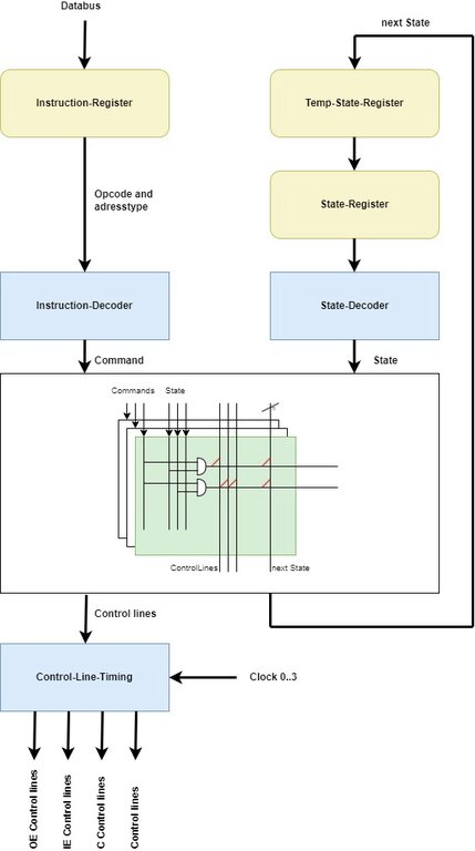
And, of course, there is not only a state register...there is also a second state register which is cleared / loaded during cycles 0 and 1. You see this detail in the structure picture and in the circuit diagram. It is the same principle than I have to use for the program counter.
The following table shows the command set of the CPU:
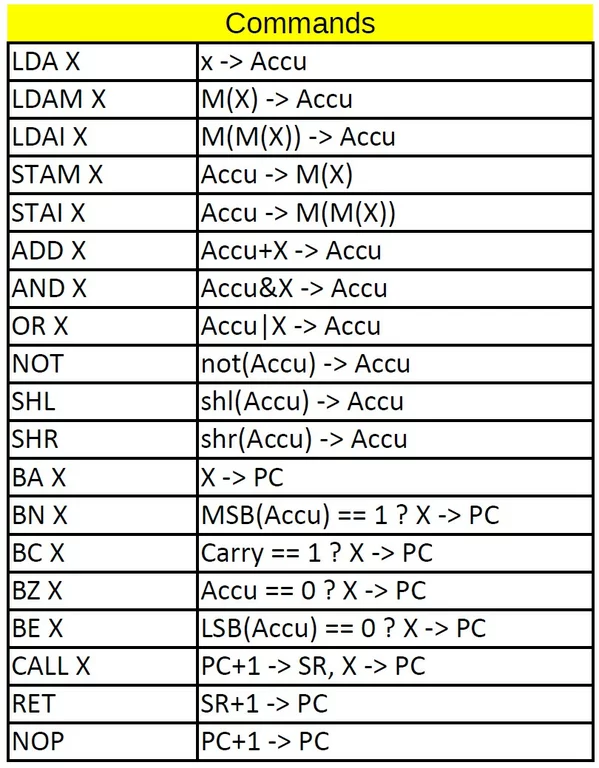
The CPU is able to adress the memory using 3 different adressing modes. a) LD X is loading the Accu with the dataword stored in the adress after the opcode, b) LD M(X) is loading the Accu with the data stored in the memory adress stored after the opcode, and c) LD M(M(X)) is ... yes, indirect adressing. The dataword after the opcode contains the adress where the CPU finds the adress of the dataword that will be stored in the Accu. Is adressing mode c) really necessary? Maybe not. But it makes it easier.
And, as you can see, a CALL / RET set of operations is also avaliable. No, there is no stack realized, only one subroutine level is possible. The return adress is stored in the register SR.
Design detail: subtraction
In the actual design, for a subtraction it would be necessary to invert the Subtrahend and add 1. This could be speed up by defining a command, a new mathematical operation.
This operation would need a multiplexer in the ALU input to distinguish between the inverted/not inverted data bus and a little logic to set the Carry of the adder for the LSB to 1.
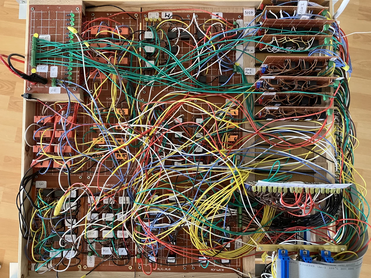
The circuit diagram
The circuit diagram of the system was designed using KiCad. The complete circuit diagram is downloadable below, the following picture set shows some of the key diagrams of the system.